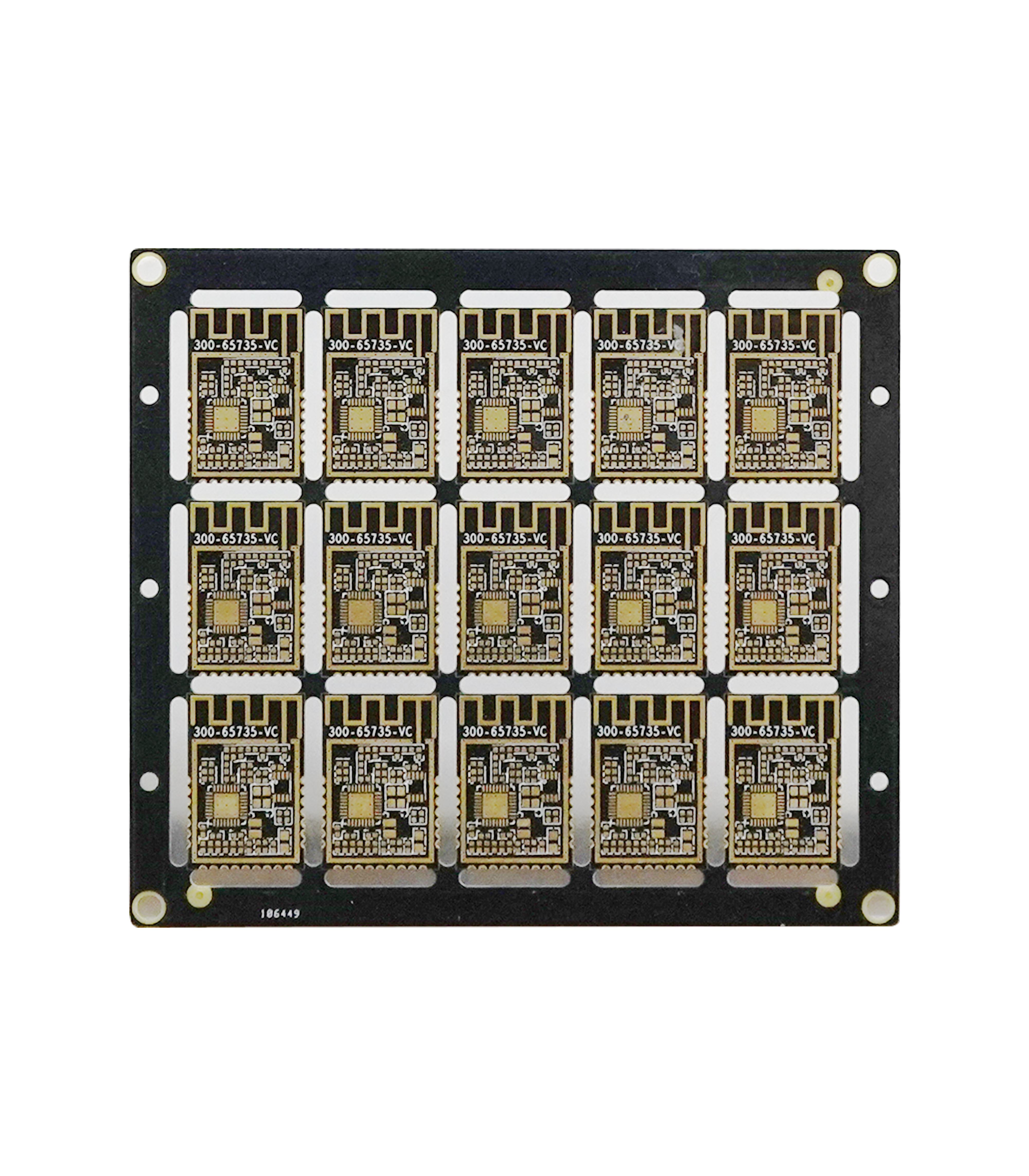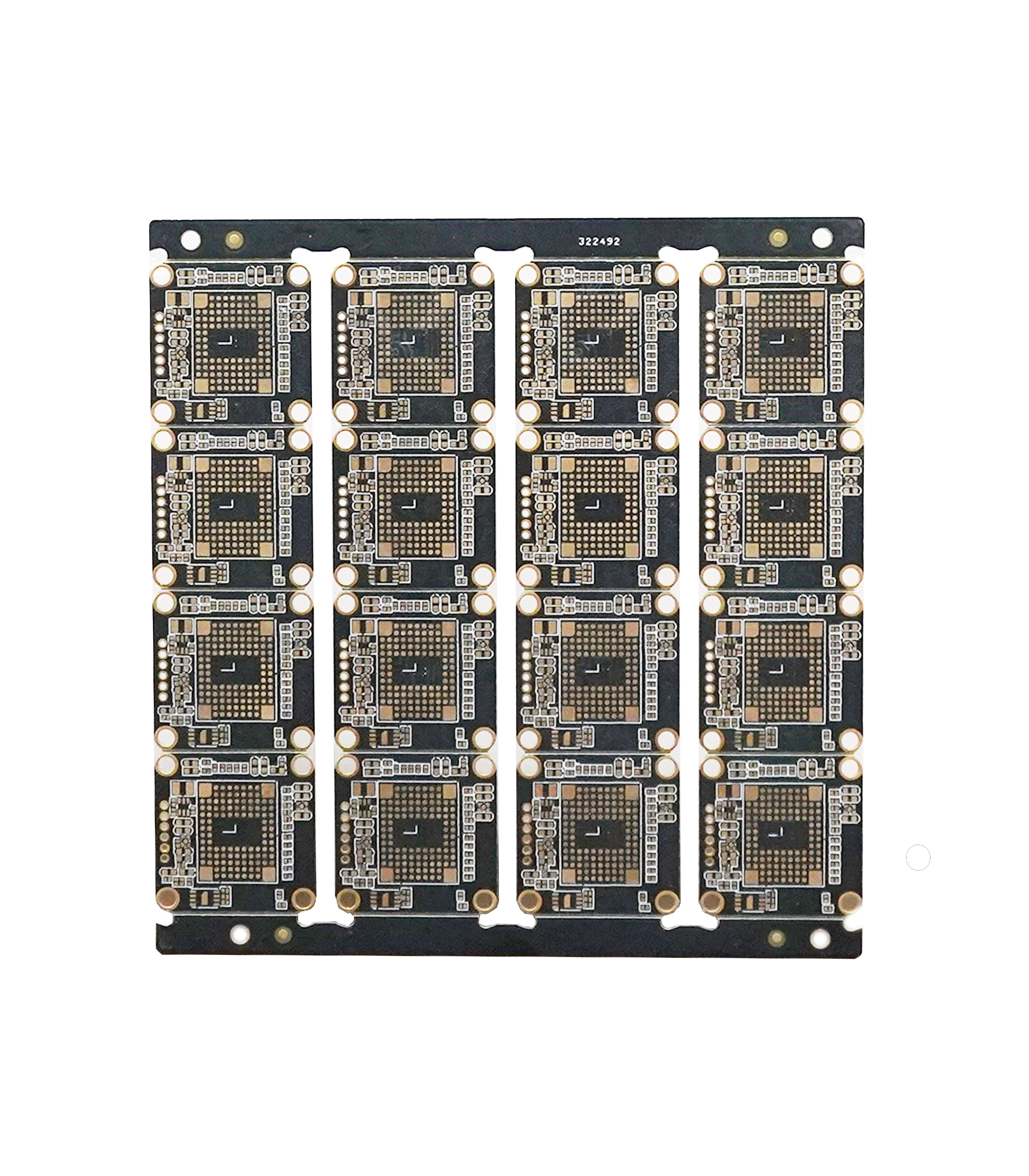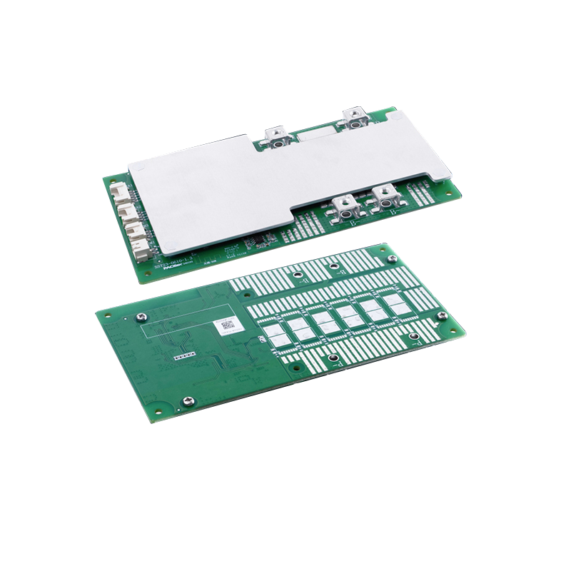
Single & Double Sided Metal Electronic Printed Circuit Board (PCB) Solid State Drive (SSD)
- PCB PCBA
| Process Specifications | Manufacturing Capabilities | Process Technology Overview |
| Layer Capabilities | 1-30 Layer | Mass Production:1-16 layers Prototype Service: 1-30 layers |
| Impedance-controlled | 2-16 Layers | With impedance tuning capability, Pricing subject to design complexity evaluation |
| PCB Material Specification | Base Material:FR-4 | Double-Sided Layers: Kingboard A-Grade Laminate,Multilayer Construction: Shengyi High-Performance Prepreg. |
| Tg Grade Specification | Range: 130°C to 180°C | ConventionalTg:135'C,Medium Tg: 150°C, High Tg: 170°C. |
| Maximum Dimensions | 53x60cm |
Panelization Max Size:54.5x62.2cm Design Limits:*Single/Double-layer: 53x60cm·Multilayer: 52.5x59cm Boards exceeding these dimensions are considered oversized Final feasibility subject to design evaluation |
| Board Thickness Specifications | 0.2-6.0mm | Thickness adiustable via lamination structure Special materials require custom procurement |
| Thickness Tolerance | Standard:+0.1mm or+10% (whichever is stricter) | For finished boards: ·≤1.0mm thickness: Strictly controlled to above tolerance ·>1.0mm thickness:Same tolerance applies |
| Drilling Specifications | 0.1-6.25MM | Laser drilling required for holes ≤0.15mm Routing process required for holes >6.25mm |
| Hole Tolerance Specifications | 0.05-0.1mm | PTH(Plated Through Hole):Diameter tolerance:+0.075mm NPTH (Non-Plated Through Hole):Diameter tolerance: +0.05mm Slot Holes (≥6.25mm):Dimensional tolerance:+0.1mm Hole Position Tolerance:Maximum deviation:+0.05mm |
| Aspect Ratio Specifications | 12:01 | Through Holes(PTH):Prototype:12:1 Mass production: 10:1 Blind Vias:1-step laser vias: 1.1 2+ step laser vias: 0.8:1 |
| Slot Width Requirements | 0.45-4.0mm | <0.45mm: Not standard (custom tooling required) >4.0mm: Must use routing process |
| Minimum Spacing Specifications | 2.8MIL(0.07mm) | Mass Production:3.0 mil(0.076mm) Prototype Production:2.8 mil(0.07mm) |
| Trace Width Tolerance Specifications | +/10%-20% | Impedance-controlled Traces:+10% Standard Traces:+20% (default when no special requirements apply) |
| Copper Thickness Specifications | 0.5-60z | Prototype Production:0.5-6 oz Mass Production: 0.5-5 oz |
| Solder Mask Specifications | Brands: Guangxin(GWT),Taiyo,Rongda | Color Selection: Red, Yellow, Blue, Green, White, Black, Purple. Matte Green
White Ink:Exclusively uses Taiyo ink (for optimal reflectivity) Matte Finish: Typically Guangxin or Rongda brands |
| Via Filling Standards | Micro-vias(<0.45mm) | According to the data, the through holes for double-sided Windows should not be blocked, those for single-sided Windows should be half-blocked, and those for double-sided Windows should be fully blocked |
| Resin Plugging Specifications | Blind vias Through holes Back-drilled holes |
Board Thickness Range:0.1-80mmHole Diameter Tolerance: Standard holes: 0.1-1.0mm Back-drilled holes: 0.15-10mm Through holes: 40:1 Blind vias: 3:1 Max variation of plugged holes on same PCB: <0.2mm |
| Gold Finger Beveling Specifications | Bevel Depth Remaining Thickness |
Bevel Angle:30-60 degrees (default 45° if unspecified)
Remaining Thickness:Client-specified(default 0.5mm) Depth:Auto-calculated based on board thickness |
| Minimum Routing Specifications | 0.8mm | Industry-standard smallest router bit diameter: 0.8mm |
| Minimum Half-hole Specifications | 0.5mm | Our Capability:Minimum finished half-hole diameter: 0.5mm |
| Special Processes | SpecialTechniques | HDl buried/blind vias、Half-hole 、Metal-edged 、Resin-filled viaStep gold fingers 、Stepped mounting holes、High-frequency PCBsAluminum substrate 、Mixed-material high-frequency laminates |
| HDl Layer Count | 1-4 Layers | Capable of manufacturing high-density interconnect (HDl) boards with blind vias upto 4 layers. |
| Process Specifications | Manufacturing Capabilities | Process Technology Overview |
| Regular Lead Time | 3-7days |
Regular Prototype 50pcs : Materials are prepared , 3 days
Small-batch Production 20-500 pcs : Materials are prepared, 5 days Batch Production 2,500 pcs : Materials are prepared , 7 days |
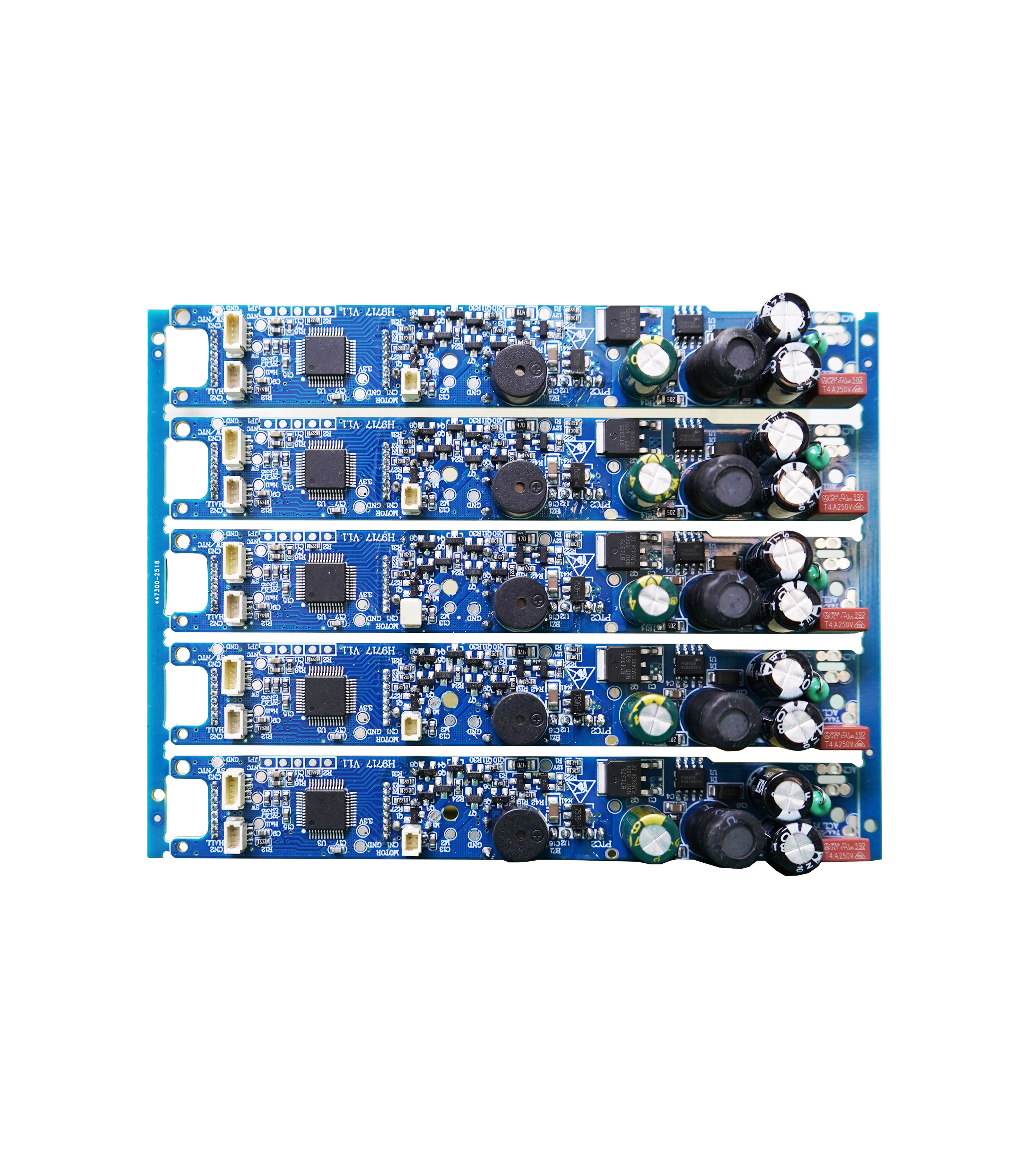
| PCBA Solder Type | PCBA,THT | |
| PCB Size | 45-1200mm | Minimum Size: 45mm × 45mm; Lower Than this size, panels need to be combined
Maximum Size: 450mm × 1200mm |
| Daily Capacity | 4 million points/days | PCBA SMT: 4 million points /day
Post-Insertion Soldering: 500,000 points/ day |
| Component Size | 0.4mm*0.2mm |
Passive Components: SMD imperial 01005 (0.4mm × 0.2mm), 0201 High-precision ICs BGA and others: X-ray inspection pitch as low as 0.25mm |
| Placement Accuracy(100FP) | 0.0375mm | |
| MOQ | 1 pcs | |
| PCB Material | FR-4, FPC, Rigid-Flex PCB, Aluminum Substrate | |
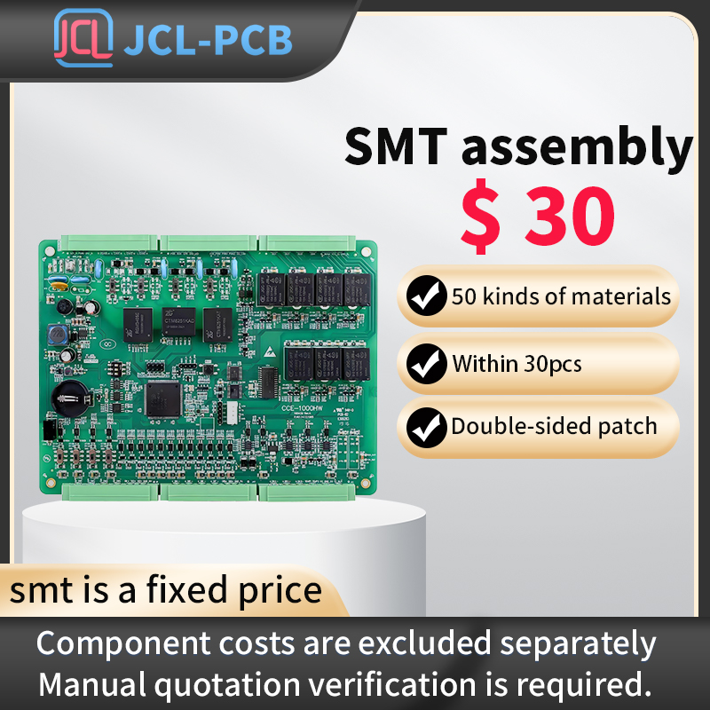
| Components serivice | Procurement Services | Full Procurement of Components
Partial Procurement of Components No Procurement |