
PCB Manufacturing & Assembly – The Essential Flow
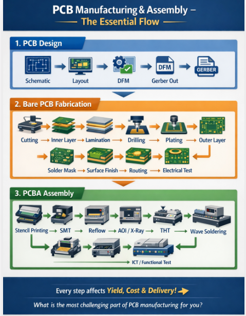
Many engineers focus on design, but do you really know how a PCB becomes a real PCBA? Here is a quick 3âstage breakdown: ð¦ 1. PCB Design Schematic â Layout â DFM â Gerber out ð§ 2. Bare PCB Fabrication Cutting â Inner layer â Lamination â Drilling â Plating â Outer layer â Solder mask â Surface finish â Routing â Electrical test ð© 3. PCBA Assembly Stencil printing â SMT â Reflow â AOI/Xâray â THT â Wave soldering â ICT/Functional test ð Every step has a direct impact on yield, cost, and delivery. ð¬ What is the most challenging part for you in PCB manufacturing? Share your experience below. #PCB #PCBA #HardwareEngineering #Manufacturing #Electronics

Post a Comment