
Silkscreen Chaos = Assembly Chaos
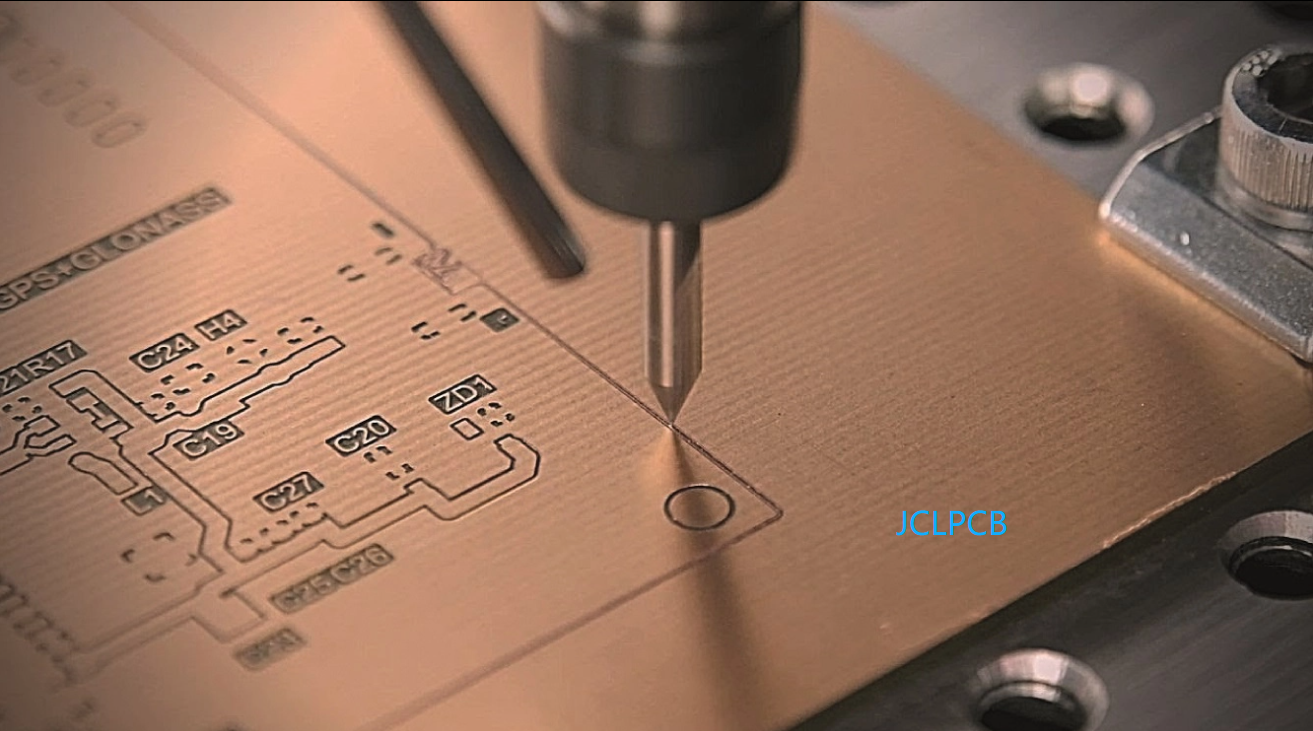
Silkscreen Chaos = Assembly Chaos ð§ Ever seen a component label printed directly on a pad? âU1â right where the solder should go â and the technician freezes. Thatâs not just annoying. Itâs a manufacturing nightmare. ð¥ What actually happens? Solder paste and silkscreen ink donât mix â Poor adhesion â Cold solder joints â Field failures Text on pads makes soldering nearly impossible â Bad joints, no test points, rework spirals out of control ð Itâs more common than you think ~10% of PCB designs still ship with this mistake. And every one of them slows down production more than youâd expect. â Simple rules that save time (and money) Keep silkscreen ⥠0.5â¯mm away from pads Text height ⥠1.0â¯mm (readable) Line width ⥠0.15â¯mm (printable) ð¡ Pro tip Silkscreen isnât decoration â itâs communication. When itâs wrong, your factory pays the price. When itâs right, your product ships faster. Have you ever seen a silkscreen blunder that stopped production? Share your story below ð #PCBDesign #ElectronicsManufacturing #DesignForManufacturing #Assembly #Engineering #Quality

Post a Comment